- 您现在的位置:买卖IC网 > Sheet目录3831 > PIC18F4423-I/ML (Microchip Technology)IC PIC MCU FLASH 8KX16 44QFN
2009 Microchip Technology Inc.
DS39755C-page 29
PIC18F2423/2523/4423/4523
The value in the ADRESH:ADRESL registers is
unknown following POR and BOR Resets and is not
affected by any other Reset.
After the A/D module has been configured as desired,
the selected channel must be acquired before the
conversion is started. The analog input channels must
have their corresponding TRIS bits selected as inputs.
To determine acquisition time, see Section 2.1 “A/D
After this acquisition time has elapsed, the A/D conver-
sion can be started. An acquisition time can be
programmed to occur between setting the GO/DONE
bit and the actual start of the conversion.
The following steps should be followed to perform an A/D
conversion:
1.
Configure the A/D module:
Configure analog pins, voltage reference and
digital I/O (ADCON1)
Select A/D input channel (ADCON0)
Select A/D acquisition time (ADCON2)
Select A/D conversion clock (ADCON2)
Turn on the A/D module (ADCON0)
2.
Configure the A/D interrupt (if desired):
Clear ADIF bit
Set ADIE bit
Set GIE bit
3.
Wait the required acquisition time (if required).
4.
Start conversion by setting the GO/DONE bit
(ADCON0<1>).
5.
Wait for the A/D conversion to complete by either:
Polling for the GO/DONE bit to be cleared
OR
Waiting for the A/D interrupt
6.
Read the A/D Result registers (ADRESH:ADRESL)
and clear the ADIF bit, if required.
7.
For the next conversion, go to step 1 or step 2,
as required.
The A/D conversion time per bit is defined as
TAD. A minimum wait of 2 TAD is required before
the next acquisition starts.
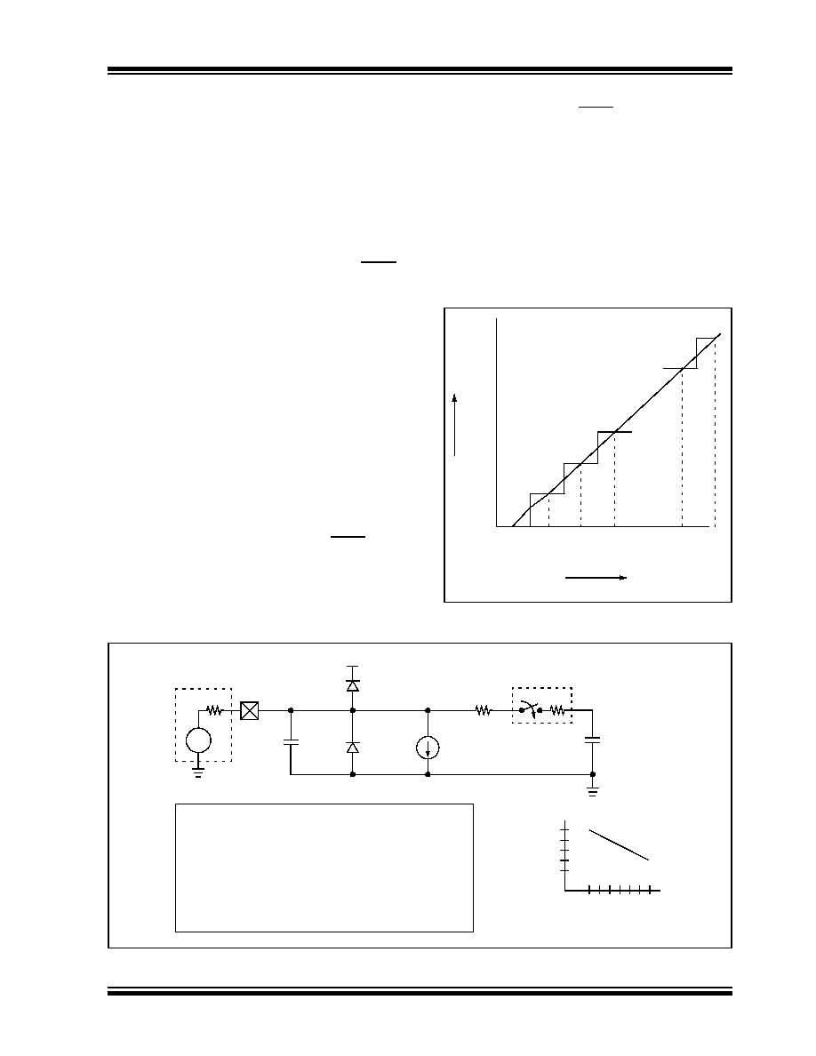
FIGURE 2-2:
A/D TRANSFER FUNCTION
FIGURE 2-3:
ANALOG INPUT MODEL
Dig
ita
lCo
d
eO
utp
ut
FFEh
003h
002h
001h
000h
0
.5
LS
B
1LS
B
1
.5
LS
B
2LS
B
2
.5
LS
B
40
94
LS
B
4
094
.5
LS
B
3LS
B
Analog Input Voltage
FFFh
40
95
LS
B
4
095
.5
LS
B
VAIN
CPIN
Rs
ANx
5 pF
VT = 0.6V
ILEAKAGE
RIC
≤ 1k
Sampling
Switch
SS
RSS
CHOLD = 25 pF
VSS
VDD
±100 nA
Legend: CPIN
VT
ILEAKAGE
RIC
SS
CHOLD
= Input Capacitance
= Threshold Voltage
= Leakage Current at the pin due to
= Interconnect Resistance
= Sampling Switch
= Sample/Hold Capacitance (from DAC)
various junctions
= Sampling Switch Resistance
RSS
VDD
6V
Sampling Switch
5V
4V
3V
2V
12
3
4
(k
Ω)
发布紧急采购,3分钟左右您将得到回复。
相关PDF资料
PIC16F874A-I/P
IC MCU FLASH 4KX14 EE 40DIP
PIC18F87J60-I/PT
IC PIC MCU FLASH 64KX16 80TQFP
PIC24HJ128GP202-I/MM
IC PIC MCU FLASH 128K 28-QFN
PIC16F873-04/SO
IC MCU FLASH 4KX14 EE 28SOIC
PIC24FJ128GA106-I/PT
IC PIC MCU FLASH 64TQFP
AT87C51RD2-RLTUM
IC 8051 MCU 64K OTP 40MHZ 44VQFP
AT87C51RD2-RLTUL
IC 8051 MCU 64K OTP 30MHZ 44VQFP
PIC16F873-04/SP
IC MCU FLASH 4KX14 EE 28DIP
相关代理商/技术参数
PIC18F4423-I/P
功能描述:8位微控制器 -MCU 16KB 768bytes-RAM 36I/O RoHS:否 制造商:Silicon Labs 核心:8051 处理器系列:C8051F39x 数据总线宽度:8 bit 最大时钟频率:50 MHz 程序存储器大小:16 KB 数据 RAM 大小:1 KB 片上 ADC:Yes 工作电源电压:1.8 V to 3.6 V 工作温度范围:- 40 C to + 105 C 封装 / 箱体:QFN-20 安装风格:SMD/SMT
PIC18F4423-I/PT
功能描述:8位微控制器 -MCU 16KB 768bytes-RAM 36I/O RoHS:否 制造商:Silicon Labs 核心:8051 处理器系列:C8051F39x 数据总线宽度:8 bit 最大时钟频率:50 MHz 程序存储器大小:16 KB 数据 RAM 大小:1 KB 片上 ADC:Yes 工作电源电压:1.8 V to 3.6 V 工作温度范围:- 40 C to + 105 C 封装 / 箱体:QFN-20 安装风格:SMD/SMT
PIC18F4423-I/PT
制造商:Microchip Technology Inc 功能描述:8-Bit Microcontroller IC
PIC18F4423T-I/ML
功能描述:8位微控制器 -MCU 16KB 768bytes-RAM 36I/O RoHS:否 制造商:Silicon Labs 核心:8051 处理器系列:C8051F39x 数据总线宽度:8 bit 最大时钟频率:50 MHz 程序存储器大小:16 KB 数据 RAM 大小:1 KB 片上 ADC:Yes 工作电源电压:1.8 V to 3.6 V 工作温度范围:- 40 C to + 105 C 封装 / 箱体:QFN-20 安装风格:SMD/SMT
PIC18F4423T-I/PT
功能描述:8位微控制器 -MCU 16KB 768bytes-RAM 36I/O RoHS:否 制造商:Silicon Labs 核心:8051 处理器系列:C8051F39x 数据总线宽度:8 bit 最大时钟频率:50 MHz 程序存储器大小:16 KB 数据 RAM 大小:1 KB 片上 ADC:Yes 工作电源电压:1.8 V to 3.6 V 工作温度范围:- 40 C to + 105 C 封装 / 箱体:QFN-20 安装风格:SMD/SMT
PIC18F442-E/L
功能描述:8位微控制器 -MCU 16KB 768 RAM 34I/O RoHS:否 制造商:Silicon Labs 核心:8051 处理器系列:C8051F39x 数据总线宽度:8 bit 最大时钟频率:50 MHz 程序存储器大小:16 KB 数据 RAM 大小:1 KB 片上 ADC:Yes 工作电源电压:1.8 V to 3.6 V 工作温度范围:- 40 C to + 105 C 封装 / 箱体:QFN-20 安装风格:SMD/SMT
PIC18F442-E/ML
功能描述:8位微控制器 -MCU 16KB 768 RAM 34I/O RoHS:否 制造商:Silicon Labs 核心:8051 处理器系列:C8051F39x 数据总线宽度:8 bit 最大时钟频率:50 MHz 程序存储器大小:16 KB 数据 RAM 大小:1 KB 片上 ADC:Yes 工作电源电压:1.8 V to 3.6 V 工作温度范围:- 40 C to + 105 C 封装 / 箱体:QFN-20 安装风格:SMD/SMT
PIC18F442-E/P
功能描述:8位微控制器 -MCU 16KB 768 RAM 34I/O RoHS:否 制造商:Silicon Labs 核心:8051 处理器系列:C8051F39x 数据总线宽度:8 bit 最大时钟频率:50 MHz 程序存储器大小:16 KB 数据 RAM 大小:1 KB 片上 ADC:Yes 工作电源电压:1.8 V to 3.6 V 工作温度范围:- 40 C to + 105 C 封装 / 箱体:QFN-20 安装风格:SMD/SMT